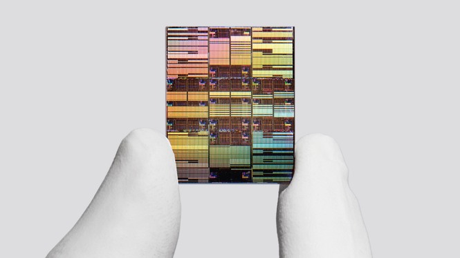
IBM has announced what it claims is the world’s first sub-1nm semiconductor technology, introducing a new 0.7nm (7 angstrom) chip architecture that could extend the fabled Moore’s Law well into the next decade.
The breakthrough comes as the semiconductor industry approaches the physical limits of traditional transistor scaling. Instead of simply making transistors smaller, IBM has developed a completely new three-dimensional transistor design called Nanostack, allowing significantly more transistors to be packed into the same area while improving both performance and power efficiency.
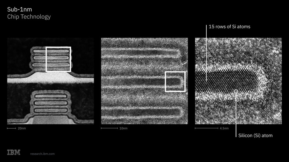
The concept involves stacking transistor layers vertically instead of placing them side by side on a flat surface. IBM says this enables significantly higher transistor density while also allowing each layer to use different semiconductor materials, letting engineers optimise performance and efficiency independently.
IBM says its experimental 0.7nm chip contains almost 100 billion transistors on a chip roughly the size of a fingernail. That’s nearly double the transistor density of IBM’s 2nm chip prototype, which was unveiled in 2021. This would allow up to 50% higher performance compared to 2nm chips at the same power level, or up to 70% lower power consumption for the same performance levels.

The company says the architecture has already been experimentally validated through working CMOS logic circuits, demonstrating that the design is capable of performing real computation.
“IBM’s latest chip breakthrough marks a landmark moment in computing, pushing technology beyond the nanometer era to the scale of atoms. With our new nanostack architecture, we’re not just making smaller transistors, we’re reinventing how chips are built to deliver dramatically more power and energy efficiency.
This industry-first innovation continues IBM’s legacy of leading in next-generation technologies and sets the foundation for the next era of computing,” – Jay Gambetta, Director of IBM Research and IBM Fellow
While the technology marks a significant research milestone, consumers shouldn’t expect sub-1nm processors anytime soon. IBM estimates that the earliest commercial production of Nanostack-based chips could begin in approximately five years, assuming manufacturing processes continue to mature.
The post IBM unveils world’s first sub-1nm chip technology appeared first on Price Shop Malaysia.